
Southeast University, Nanjing 211189, China
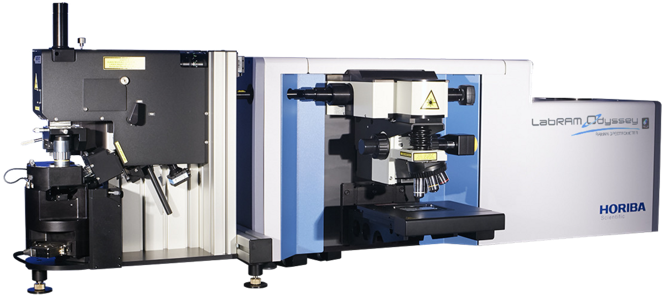
LabRAM Odyssey Nano
-
Overview
TERS imaging is performed with an AFM-Raman system, where a Scanning Probe microscope (SPM that can be used in atomic force, scanning tunneling, or normal/shear force mode) is integrated with a confocal Raman spectrometer through an opto-mechanical coupling. The scanning probe microscope allows for nanoscale imaging, the optical coupling brings the excitation laser to the functionalized tip (or probe), and the spectrometer analyzes the Raman (or otherwise scattered) light providing a hyperspectral image with nanometer scale chemical contrast.
A TERS system is based on a metallic tip (generally made of gold or silver) employed to concentrate the incident light field at the apex. The tip acts as a nano-source of light and local field enhancer, greatly improving the Raman sensitivity (by a factor of 103 -107) and reducing the probed volume to the “nano” region immediately below the tip.
Features
In combination, the two techniques yield an attractive and unique tool for entering the nano-world. With over a decade of experience in this exciting new field, we have refined the technique to its utmost with uncompromised performance to bring you a tool that is not only extremely powerful and versatile, but is also so easy to use, fast and reliable that generating outstanding data is virtually effortless.MULTI-SAMPLE ANALYSIS PLATFORM
Macro, micro and nano scale measurements can be performed on the same platform.HIGH COLLECTION EFFICIENCY
Top-down, oblique and bottom Raman detection for optimum resolution and throughput in both co-localized and tip-enhanced measurements.HIGH SPECTRAL RESOLUTION
Ultimate spectral resolution performance, multiple gratings with automated switching, wide spectral range analysis for Raman and Photoluminescence.
HIGH SPATIAL RESOLUTION
Nanoscale spectroscopic resolution (down to 10 nm) through Tip-Enhanced Optical Spectroscopies (TERS: Tip-Enhanced Raman Spectroscopy and TEPL: Tip-Enhanced Photoluminescence).
MULTI-TECHNIQUE / MULTI-ENVIRONMENT
Numerous SPM modes including AFM, conductive and electrical modes (cAFM, KPFM), STM, liquid cell and electrochemical environment, together with chemical mapping through TERS/TEPL. Full control of the two instruments through one workstation and a powerful software control, SPM and spectrometer can be operated simultaneously or independently.
HORIBA Jobin Yvon LabRAM HR Raman system
-
Overview
The LabRAM HR systems provide high spectroscopic resolution and a unique wavelength range capability that offers both great flexibility and high performance. They are widely used for standard Raman analysis, photoluminescence (PL), tip enhanced Raman scattering (TERS) and other hybrid methods.
-
Features
High spectral resolutionThe unique high resolution mode is ideal for subtle band analysis such as that for phase (crystalline/amorphous), of proteins, weak bonding forces (such as hydrogen bonding) and semiconductor stress measurements – in fact most applications where it is important for the precise characterization of position or shape of the Raman spectral features. Band analysis with a resolution in the order of 0.3 cm-1 to 1 cm-1 is particularly suited to the high resolution mode. Its dual capabilities also enable more routine low/medium resolution Raman analysis and even broader band laser induced micro-fluorescence or luminescence to be conducted on the same bench-top instrument.
True confocal performance
The LabRAM HR has a true confocal pinhole with user controlled variable aperture. Unlike pseudo-confocal configurations (e.g., slit-binning methods) the confocal pinhole fully matches the laser spot and provides the highest spatial resolution with maximum signal throughput.UV, visible and NIR capability
The LabRAM HR can be configured with the unique Dual Path Optics to allow UV-visible-NIR sensitivity without compromise. Unlike achromat (lens) based systems the Dual Path Optics offers fast, simple switching between UV and VIS/NIR regions. No adjustment or alignment is required.Integrated upright, inverted and free space microscopes
Different applications can be best served with different microscopes – for this reason, the LabRAM HR can be configured with standard upright, inverted or free space microscopes.- The upright microscope is the standard option for materials analysis, and widely used for Raman analysis in many varied fields.
- The inverted microscope is ideally suited for life science research, where tissue and live cells are frequently analysed within culture media.
- The free space microscope provides a unique level of access to samples. The bottom frame is removable so that it offers a large free space beneath the microscope objective turret. Large cryostats, (e.g., liquid Helium cooled), sample environment equipment (diamond anvil cells) and similar devices can be accommodated with this microscope.
- Dual microscope options are also available (for example, upright + inverted) – these allow the benefits of different configurations to be available on a single Raman instrument.
Fast Raman imaging
With the SWIFT™ and DuoScan™ fast Raman imaging technologies the LabRAM HR allows the collection of large area Raman images in the matter of seconds/minutes. The unique combination of innovative optics, detectors and software combine to provide true confocal Raman imaging with an unmatched speed of data acquisition.
XploRA™ Desktop Confocal Raman Microscope
-
Overview
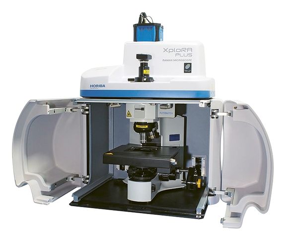
Xplora plus is an intelligent fully automatic micro Raman system, which integrates many unique functions. It not only has excellent performance, but also is convenient to use and fast to analyze. It is very suitable for multi-user operation and switching analysis of various samples. It is an ideal choice for research work and Analysis Center. Xplora plus is equipped with a unique swift fast imaging function, which can realize ultra fast confocal Raman imaging, which is 10 times faster than ordinary imaging speed. The true confocal design ensures high-quality imaging quality and spatial resolution even under ultra fast imaging conditions. In addition, Xplora plus has unparalleled scalability, such as polarization Raman, particle analysis and Raman AFM.
-
Features
Xplora plus is a high-performance and compact Raman spectrometer with microscopic confocal function based on the simple and easy-to-use design concept and user's operation habits, and integrated with a variety of intelligent functions.
- Swift TM ultra fast imaging function
- High sensitivity
- True confocal performance
- Complete optical microscope performance
- Optimized resolution, multiple spectrum acquisition ranges
- HORIBA's unique OneClick Raman analysis
- NIST (National Institute of standards and Technology) certification, patent automatic calibration technology
- Excellent optical stability - providing reliable long-term detection
- Automatic operation
- System expansion
- Raman and AFM combined with ters (needle tip enhanced Raman)
- Multiple excitation wavelengths - applicable to all kinds of samples and optimized experimental results
- Professional Raman database - rapid identification and analysis
HORIBA Jobin Yvon Fluorolog-3 Spectrofluorometer

-
Overview
The FluoroLog®-3 is a unique, modular system which allows the researcher to interchange a versatile range of accessories to correspond perfectly with the characteristics of a given sample. From analysis of steady-state or molecular dynamics to IR probes, the FluoroLog®-3 comes equipped with a wide range and limitless configuration of accessories to enhance the accuracy and speed of your application.
-
Features
- World’s most sensitive spectrofluorometer *
- Can detect 50-femtomolar fluorescein
- Unique, modular system adapts to new experiments or changing techonolgy so is never obsolete
- Interchange wide range of computer-controlled accessories: spectrometers, detectors, sources, and more!
- Totally computer-controlled
- All-reflective optics so that the sample is in focus at all wavelengths
HITACHI U-3900 UV-Visible Spectrophotometer
- Possible to perform measurements in a wide absorbance range with low stray light and low noise.
The larger the amount of transmitted light, the lower the noise of the obtained absorption spectrum so that a wider absorbance range can be measured. Measurements of high concentration samples can be performed over a wider concentration range. - Stable spectrometer with double beam optical system
The light source uses a WI lamp (visible range) and a D2 lamp (ultraviolet range) that switches wavelength depending on the measurement. The double beam system divides the monochromatic light so that the diffraction grates into the control and the sample with a rotational mirror, guiding the light to the sample chamber.
Single Monochrome Type U-3900 uses a spherical surface mirror in front of the entrance slit, while the Double Monochrome Type U-3900H uses diffraction grating. - UV Solutions for U-3900 (PC connected) allows for easy device control and supports various quantitative-analysis functions.
Special operation software that offers substantial functions such as measurement data comparison and a preview function that allows for a more powerful analysis.Item U-3900 U-3900H Monochromator Diffraction grating
Single monochromator
Seya-Namioka mountDiffraction grating-diffraction
grating Double monochromator
Seya-Namioka mountWavelength range 190 to 900 nm Spectral bandpass 0.1, 0.5, 1, 2, 4, 5 nm (6 steps) Wavelength accuracy ±0.1 nm (at 656.1 nm after wavelength calibration)
OptiFDTD
OptiFDTD 10.0is a powerful, highly integrated, and user friendly CAD environment that enables the design and simulation of advanced passive and non-linear photonic components.
OptiFDTD enables you to design, analyze and test modern passive and nonlinear photonic components for wave propagation, scattering, reflection, diffraction, polarization and nonlinear phenomena. The core program of OptiFDTD is based on the Finite-Difference Time-Domain (FDTD) algorithm with second-order numerical accuracy and the most advanced boundary conditions – Uniaxial Perfectly Matched Layer (UPML).
The algorithm solves both electric and magnetic fields in temporal and spatial domain using the full-vector differential form of Maxwell’s coupled curl equations. This allows for arbitrary model geometries and places no restriction on the material properties of the devices.
MSP-300CT Magnetron Sputtering System
-
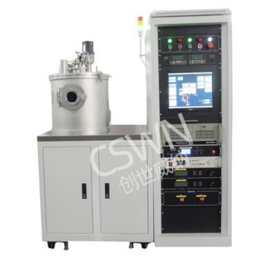
This equipment can be used for the preparation of single film, multilayer film, co-sputtering film, noble metal film, semiconductor film, dielectric film, magnetic film, heat-resistant alloy film, hard film, etc.
-
Specifications:
-
Item Parameter Power supply DC power supply x2 set and RF power supply x1 set Control method PC automatic control Sputtering path Upward Process gas 2 routes gas flow Ultimate vacuum ≤ 1.0 x10⁻⁵ Pa Sputtering target φ50 mm x3 set Substrate temperature Room temperature~600 ℃ Uniformity of film thickness With the scope of φ50 mm≤ ±5.0 %
MNT Single Chamber Type ALD

-
The MNT-S ALD system equipped with ozone generator and visual operation interface. Could be used to deposit conventional oxide films, copper, TiN , etc. There are water source, aluminum source, molybdenum source and silicon source ,respectively.
-
Specifications:
-
MNT-S ALD sample chamber size: 12 inches Substrate heating temperature: RT-400℃;1℃ Number of precursor paths: 4 ways Pipeline temperature of
precursor source:RT-200℃;1℃ Source vessel temperature: RT-200℃;1℃ Depositional model: Fast mode, high depth ratio mode, professional doping mode
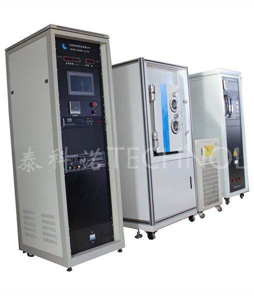
High Vacuum Electron Beam Evaporator TEMD500
-
Application
Colleges, universities, research institutes and enterprises for scientific research and small batch preparation of new thin film materials.
-
Features
- Integrated equipment design, small footprint, high cost performance, stable performance, low maintenance cost.
- It is suitable for the preparation of metal element films, semiconductor films, and organic films in the laboratory, and can also be used for the preliminary process test of the production line.
- Suitable for the preparation of optical films, conductive films, semiconductor films, ferroelectric films, etc.
Specifications:
-
Item Parameter Vacuum chamber structure Vertical cylindrical side opening structure, rear exhaust system Vacuum chamber size Φ500 × H650 mm Heating temperature Room temperature~300 ℃ Rotating substrate stage Flat type Φ200 mm Uniformity of film thickness ≤ ±5.0 % Kaufman ion source Optional Evaporation source Electron gun 8 KW, 6-cavity crucible, domestic and imported optional, with 3-3 groups of resistance evaporation Control method PLC + touch screen man-machine interface semi-automatic control system Area Length × Width L2500 × W1600 mm Total power ≥ 17 KW