Research Interest
The research at the Spectroscopy and Optoelectronics group is mainly focused on spectroscopic investigation, laser micro/nano manufacture, modulation of the optical properties of low dimensional materials, and the application in optoelectronic devices.
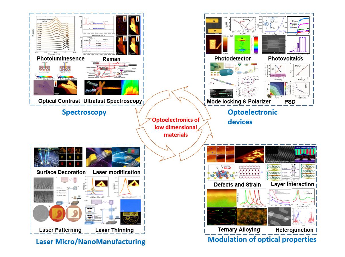
1. Spectroscopic investigation of low dimensional materials
Optical spectroscopies are powerful techniques for the studies of low dimensional materials. They are efficient and nondestructive, and the spatial resolutions can be varied from the submicrometer to centimeter range by manipulating the focused laser beam. We have developed an optical contrast spectroscopy technique to precisely identify the thickness of two dimensional materials (up to 10 layers). We adopt Raman and photoluminescence (PL) spectroscopy to investigate the defects, doping, and electronic band structures of low dimensional materials. Ultrafast spectroscopies including time-resolved PL and optical pump-optical/THz probe spectroscopies are also employed to investigate the carrier dynamics and photoelectrical properties of low dimensional materials.
References:
1. Ni ZH et al. Graphene thickness determination using reflection and contrast spectroscopy Nano Letters 07, 2758 (2007)
2. Ni ZH et al. On resonant scatterers as a factor limiting carrier mobility in graphene Nano Letters 10, 3868-3872 (2010)
3. Liu HW et al. Composition-dependent electron transport in CdSxSe1-x nanobelts: a THz spectroscopy study Optics Letters 39, 567-570 (2014)
4. Wu ZT et al. Defects as a factor limiting carrier mobility in WSe2: a spectroscopic investigation Nano Research 9, 3622 (2016)
2. Modulation of the optical properties of two dimensional materials
There is a great need for controlling the properties of two dimensional (2D) materials to fulfill the requirements of various applications. In the field of optoelectronics, e.g. photodetections, the materials are expected to have finite bandgap, high mobility and strong optical absorption. We are focused on the modulation of the optical properties of graphene and other 2D materials through the control of interlayer interactions, edge-chirality, strain and defect engineering, and so on.
References:
1. Ni ZH et al. Tunable stress and controlled thickness modification in graphene by annealing ACS Nano 2, 1033 (2008)
2. Liu YL et al. Layer-by-Layer Thinning of MoS2 by Plasma. ACS Nano 7, 4202 ( 2013)
3. Nan HY et al. Strong Photoluminescence Enhancement of MoS2 through Defect Engineering and Oxygen Bonding ACS Nano 8, 5738 (2014)
4. Lu JP et al. Bandgap Engineering of Phosphorene by Laser Oxidation toward Functional 2D Materials ACS Nano 9, 10411-10421 (2015)
3. Laser micro/nano manufacture
Considering the small size, precisely handling of the materials is a challenging issue which restricts the practical applications of low dimensional nanomaterials. With the specific features of high spatial resolution, high energy density, flexibility, and so forth of lasers, the laser micro/nano manufacturing techniques are expected to work as a versatile tool for the manipulation, structural transformation, micropatterning and chemical modification of low dimensional nanomaterials. We have devised, fabricated and optimized the laser manufacturing technique to realize laser patterning, thinning, modification and surface decoration on the low dimensional nanomaterials.
References:
1. Lu JP et al. Improved Photoelectrical Properties of MoS2 Films after Laser Micromachining ACS Nano8, 6334-6343 (2014)
2. Lu JP et al. Atomic healing of defects in transition metal dichalcogenides Nano Letters 2.15, 3524-3532 (2015)
3. Lu JP et al. Microlandscaping of Au Nanoparticles on few-layer MoS2 films for Chemical Sensing Small 11, 1792-1800 (2015)
4. Lu JP et al. Enhanced Photoresponse from Phosphorene-Phosphorene-Suboxide Junction Fashioned by Focused Laser Micromachining Advanced Materials 28, 4090-4096 (2016)
4. Optoelectronic properties and devices
One of the most promising applications of 2D materials is optoelectronic device, including photodetection, light emitting and photovoltaic devices. Together with our collaborators, we have developed a series of 2D materials based optoelectronic devices, e,g, graphene based mode-locking laser and optical polarizer, high performance photodetectors as well as position sensitive detectors.
References:
1. Wang WH et al. High performance position-sensitive-detector based on graphene-silicon heterojunction Optica 5, 27-31 (2018)
2. Guo XT et al. High-performance graphene photodetector using interfacial gating Optica 3, 1066-1070 (2016)
3. Lu JP et al. Hybrid Bilayer WSe2 -CH3NH3PbI3 Organolead Halide Perovskite as a High-Performance Photodetector Angewandte Chemie International Edition 55, 11945-11949 (2016)
4. Wang WH et al. Interfacial amplification for graphene based position sensitive detectors Light: Science & Applications 6, e17113 (2017)